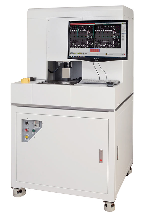
Finished product inspection (printed circuit board)
Parameter setting is easy, set the parameters time is less than 5 minutes, get the new part no. to start inspection, no more than 5 minutes.
Smaller system dimensionSmaller system dimension which won’t waste the install area and suitable for pre-shipment sampling and suitable for pre-purchase sampling.
Inspection the type of defectOur company has been independent development of software, with more than 20 years of experience, even after the sale of products, but also continue to help customers update the software and optimize the system.
To determine defect by user's parameters and system embedded logic. Simple operation and no need reference required
Function of laser marking defectsMarking defect distribution location, laser indicator, output defect distribution map, coordinate's file.
Inspect defects on the PCB by optical lens capturing system. The inspection system can reduce damages and promote product quality.
Analog microscope to take the principle of image, the use of high-energy front projection, side projection light source to be detected, through the precision optical lens group, focusing to the top of the high-resolution sensor system to obtain images, and then use the computer to convert the image into digital values, then use the following model to identify defects.