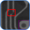
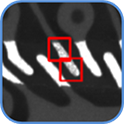
There is an open circuit under the solder mask layer.
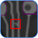
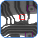
There is a short circuit which was polluted under the solder mask layer.
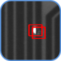
Solder mask scratches, the width of the scratches not be less than 15um.
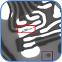
Solder mask surface was damaged, line damaged, copper exposure, the image appears white part.
The covering position of the solder mask is shifted so that solder mask opening is insufficient.
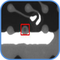
Via fill depth is insufficient, the image will show the color difference.
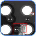
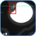
There are foreign objects on the solder mask, so that the image has a three-dimensional sense.
Solder mask opening is contaminated and the residual copper slag may cause a short circuit.
Solder mask opening is broken or there is a foreign material inside, the picture looks like a round hole.
When the thickness of nickel is insufficient, it will affect the gold-plated after the good or bad, it is much rough.

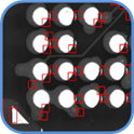
According to the requirements of customers, set the space of the bond-finger, when inspect the lack of space, the software will marking.
Solder mask opening by the external damage, image is white gold face, but it is black.

According to the requirements of customers, set the width of the bond -finger, when inspect the lack of width, the software will mark out.